Russia creates its first 130 nm lithography tool, which lags 25 years behind Western counterparts

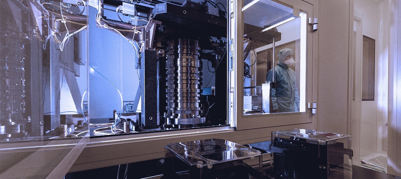
Zelenograd Nanotechnology Center (ZNTC) has completed the third stage of R&D on Russia's first lithography tool for 200-mm wafers on a 130nm process. CNews reported the news back in August 2026. The prototype is now undergoing internal testing, and it will be years before a real fab can use it for mass chip production.
Blogger Dmitrii Kuznetsov called the tool the "first Russian 130nm-capable lithograph" built from domestic components. The documents seen by journalists paint a more complicated picture.
ZNTC is the lead contractor, but the lithography system itself was developed by Belarus-based Planar, which backs up earlier reports about the program.
Responsibilities were split like this:
Planar developed the lithography system, manufactured mechanical assemblies and components, and handled commissioning of the prototype
Lassard built the lasers for the unit
ZNTC handled development of the overall system, design of test and process equipment, projection-lens calculations, and process modeling and development
Russia's Ministry of Industry and Trade allocated about 5.7 billion rubles ($70 million) for the entire program.
One ZNTC 130nm stepper is estimated to cost around $6.7 million, with another $600,000 or so for the laser light source. Together, a single tool comes to $7.3 million. The stepper works on a step-and-repeat principle, exposing the wafer section by section with a sequential shift rather than all at once.
For comparison, the ASML PAS 5500/150 i-line stepper, designed for 0.35-micron nodes, cost $3.1 million at launch in Q1 2001. With cumulative inflation of about 88%, that comes to roughly $5.8 million in 2026 dollars. The Russian machine, meanwhile, handles 200-mm wafers and is built for 130nm.
Intel adopted the 130nm process in 2001 and AMD followed in 2002, which is where the gap of about a quarter century comes from. Russian chipmakers have historically developed two 130nm-class nodes, but both rely on ASML lithography equipment. Whether the ZNTC stepper can be integrated into existing process flows is still unclear.
ZNTC says it is also responsible for process "modeling and development." That most likely means not building a full 130nm technology from scratch, but tuning the lithographic process around this particular machine. The work covers a long list of parameters:
resist and exposure dose
focus and process window
masks
alignment and overlay
develop conditions and temperatures
The tool is now going through internal engineering and acceptance testing. After that, ZNTC will have to finalize the design and validate all key characteristics, from imaging quality and overlay accuracy to reliability and throughput, which will take well over a year.
Only then will prototype machines reach actual chipmakers. They will need to characterize the equipment and qualify it for their production lines, which will take months, if not years.
A realistic timeframe for the Russian tool to start processing commercial wafers is 2029 at the earliest, according to estimates. Limited production of the steppers themselves could begin sooner if ZNTC has all the required parts, but that doesn't mean they are ready for volume semiconductor manufacturing.
- I've launched Skyrim with the first snow for 15 years in a row – gamers were surprised by a man from the Urals who has snow outside his window in October
- Schoolboy destroyed a 26-million-ruble IMAX screen with a bubble tea ball